|
|
|
FPGA-CPU Communication via an External Memory Interface
Jan 2017 - Mar 2017
Overview
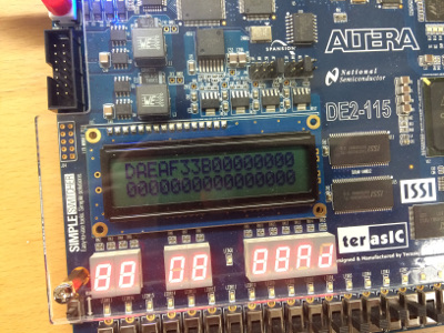
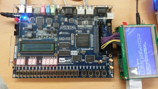
Implementation of a FPGA-CPU bridge for communication between a TI AM1808 ARM CPU and an Altera FPGA over the exposed EMIFA bus on the ARM CPU, which provides an interface of synchronous & asynchronous RAM, as well as DMA channelsupport. In the end, we were able to verify successful write operations to the FPGA, however, we were unsuccessful at read operations.
Keywords: FPGA, Embedded CPU, Micro-Processor, MPU, ARM, EMIF, C, GCC
Tasks
- Paired Programming.
- Debugging with teammate.
- Oscilloscope Probing of pins.
- Presentations of project.
- Team Meetings.
- Wrote Weekly Updates.
- Contributed to Paper.
Technologies Used
- FPGA (Altera Cyclone IV)
- ARM CPU (TI AM1808)
- EMIF
- 500 Mhz Oscilloscope
- C
- GCC
Paper
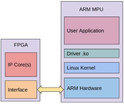
Many embedded devices are designed around the concept of heterogeneous computing for both speed and power consumption reasons. Often this will lead to systems containing a primary compute unit (a CPU), and a secondary compute unit that acts as a co-processor, where the two are connected through some variant of a system bus. The most notable example of this would be the standard CPU-GPU model seen in laptop and desktop computers. In more specialized cases, such as test instrumentation, the model will often take the form of CPU-FPGA, where the primary compute unit is a low power embedded processor. In the context of test instrumentation, this model allows for real-time data streaming from sensors to be processed by the FPGA, and then presented to the user by way of the CPU. The design and implementation of such a system, however, is non-trivial, requiring custom software solutions to properly bridge the CPU-FPGA gap.
Read More